Crucibles: Importance in VGF and MBE Growth of Semiconductors")
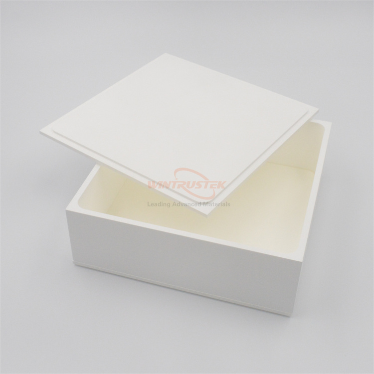
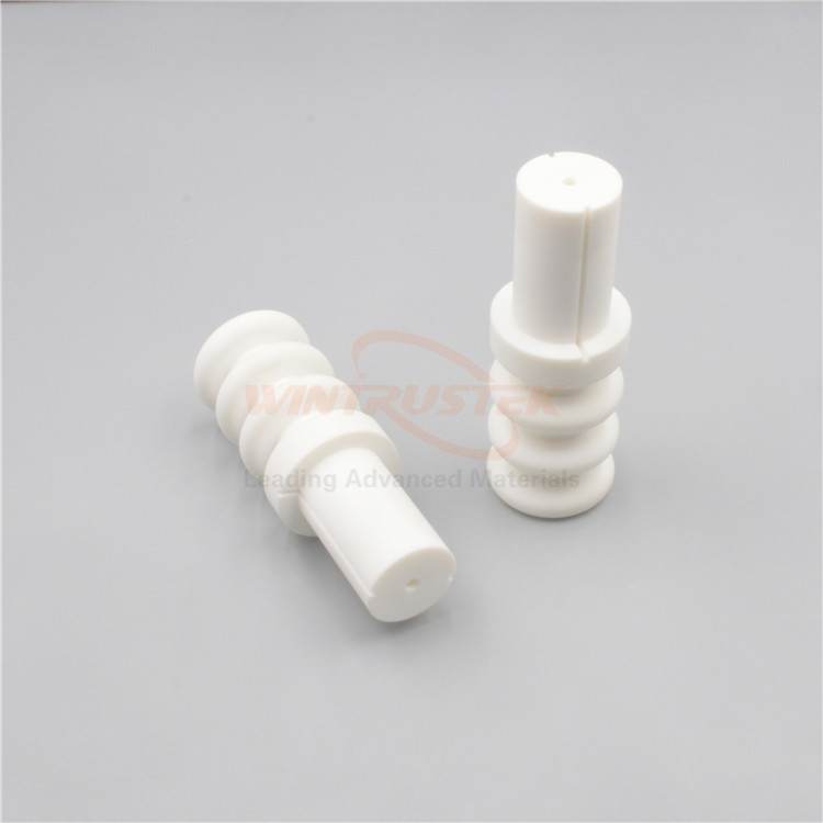
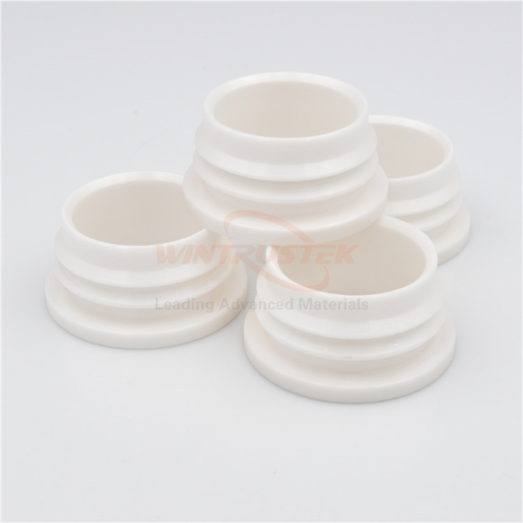
(PBN VGF Crucible produced by Wintrustek)
Manufacturing high purity compound crystals such as Gallium Arsenide (GaAs), Indium Phosphide (InP) and Gallium Nitride (GaN) for the semiconductor industry is an exercise in accuracy. The approach utilizes two advanced crystal growth techniques, the Vertical Gradient Freeze (VGF) and the Molecular Beam Epitaxy (MBE). These processes operate under severe high-vacuum and ultra-high-temperature conditions, therefore the choice of crucible material is never trivial - it can literally make or break the purity of the final wafer.
Older applications may use normal graphite or quartz vessels but today’s stringent requirements call for a unique material: Pyrolytic Boron Nitride (PBN).
At Wintrustek, we are experts in high-performance ceramic solutions for the electronics industry. We know that PBN crucibles are not only containers but are important components that directly influence electronic mobility, crystal structure integrity and production yield.
So why have PBN crucibles become indispensable for VGF and MBE semiconductor crystal growth? Let’s take a closer look.
1. Ultra High Chemical Purity: Remove Source Contamination
Chemical inertness is the absolute minimum criterion for any substance in contact with molten semiconductors. Gallium and indium melt at temperatures where common crucible materials may progressively degrade or react and contaminate the melt with trace impurities such as silicon, oxygen or carbon. Even at parts per billion (ppb) levels, contamination in compound semiconductors can alter the lattice structure and affect electrical performance.
PBN is prepared via a chemical vapor deposition (CVD) technique, yielding a monolithic material with a purity level surpassing 99.999%. There are practically no binders or catalysts, such that nothing leaches into the semiconductor melt.
Furthermore, PBN has a highly aligned layered hexagonal crystal structure and is non-porous unlike sintered boron nitride. The fully non-porous substance repels moisture, ambient gasses and process residues to ensure an uncontaminated environment from one development cycle to the next.
2. Good Resistance to Corrosion by Aggressive Melts
The crucible is used for development of VGF crystals in hostile elemental melts at temperatures often in excess of 1200 °C for days at a time. Corrosiveness is also a known property of molten metals (especially gallium) which can moisten and dissolve most metallic and ceramic matrices.
PBN is very resistant to chemical attack by molten metals and acids. The special anisotropy of the material causes the crystal planes to run parallel to the crucible surface, forming a smooth, non-wetting barrier.
The Non-Wetting Advantage: Since the molten compound does not wet or adhere to the PBN walls, the solidified ingot can be simply released following the VGF cooling phase. This removes mechanical stress on both the pricey crucible and the newly formed crystal ingot, greatly increasing manufacturing yields.
The Wintrustek Standard Wintrustek controls the CVD layering orientation during manufacturing to produce PBN Crucibles with ultra-smooth surface finishes and uniform wall thicknesses suitable for large diameter VGF crystal pullers for easy demolding and long component life.
3. Excellent Thermal Shock Resistance and Thermal Anisotropy
Both the VGF and MBE techniques include quick temperature profiling of components. PBN crucibles for MBE effusion cells must survive rapid heat shocks up to 1400°C in ultra-high vacuum (UHV) without breaking or outgassing.
Due to the layered atomic structure of PBN, it has certain interesting thermal characteristics:
Thermal Shock Resistance Can be cycled repeatedly via extreme temperature differentials without thermal stress fractures.
Thermal Anisotropy: PBN conducts heat more faster in the "A" direction (parallel to the surface) than in the "C" direction (perpendicular, through the wall thickness). This unusual characteristic helps to smooth localized hot spots, leading to a very uniform temperature profile over the molten source inside an MBE effusion cell. Then it has to be heated uniformly to have a stable and predictable evaporation rate of the molecular beam.
4. Mechanical Robustness of Thin-Walled Structures
PBN is produced via vapor deposition, layer by layer, rather than pressing and sintering, therefore it can be made into ultra-thin walled structures, commonly between 0.8 mm and 1.5 mm thick, while yet having great mechanical strength.
Such narrow walls allow the maximum capacity for the raw material charge, and rapid responsive thermal management from the external heating sources in MBE systems when space within the effusion cell is at an absolute premium.
Summary: PBN Operational Advantage Matrix
Below, Wintrustek summarizes the comparative material benchmarks to show the functional shift to PBN:
| Performance Property | Quartz / Silica | Boron Nitride (BN) | Pyrolytic Boron Nitride (PBN) |
| Purity Level | Moderate (~99.9%) | Low-Moderate (Contains oxide binders) | Ultra-High (>99.999% CVD Purity) |
| Porosity | Non-porous | Porous (Absorbs moisture/gasses) | Completely Impermeable (Zero Porosity) |
| Melt Wetting | Highly reactive with molten metals | Moderate wetting tendencies | Non-wetting (Easy crystal ingot release) |
| Thermal Behavior | Prone to devitrification at high temperatures | Isotropic thermal transfer | Anisotropic (Ensures highly uniform heat zone) |
| UHV Outgassing | Low | High (Outgasses trapped impurities) | Virtually Zero (Perfect for MBE systems) |
Wintrustek for Critical Semiconducting Materials
With the shrinkage of the semiconductor nodes and the increasing requirement for defect free wafer substrates, the dependency on high-tier manufacturing consumables such as PBN crucibles becomes absolute. Whether you grow large diameter GaAs/InP ingots using VGF or do precision thin film deposition in MBE effusion cells, a trusted materials partner is essential to maintaining high batch to batch yield.
Wintrustek produces high purity PBN crucibles, VGF tubes, and specialized effusion cell components for the demanding requirements of modern wafer manufacturing.
Contact Wintrustek immediately at sales@wintrustek.com to discuss your application with our engineers, explore unique dimensions and obtain premium material solutions for your semiconductor growing infrastructure.