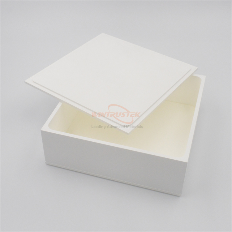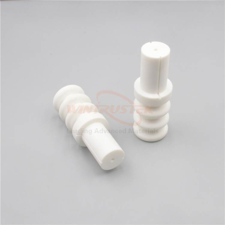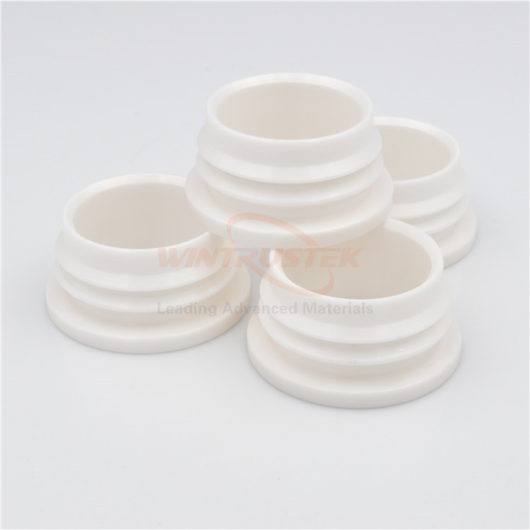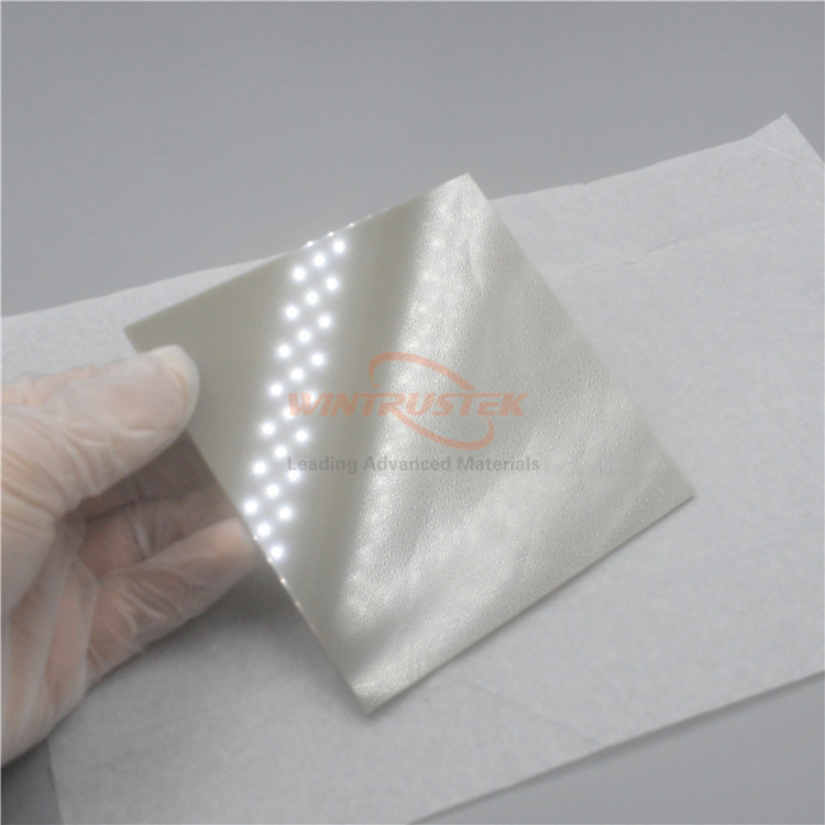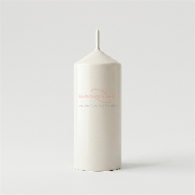
(Pyrolytic Boron Nitride VGF Curcible)
With the booming development of AI computing power, 800G/1.6T optical modules and photonic integrated circuits (PICs), Indium Phosphide (InP) is one of the most important III-V compound semiconductor materials. InP substrates are important for the fabrication of high-speed lasers and photodetectors due to their high electron mobility and straight bandgap.
However, the growth of high-quality, large diameter InP single crystals using the methods such as Vertical Gradient Freeze (VGF) or Liquid Encapsulated Czochralski (LEC) involves outstanding engineering hurdles. The vapor pressure of the phosphorus element is very high at high temperatures and the thermal field and melt composition are easily unstable.
To get over these problems of manufacture, Pyrolytic Boron Nitride (PBN) crucibles are now the typical vessel for the formation of InP single crystals.
Wintrustek is a specialist in precision CVD ceramics designed for advanced semiconductor fabrication. Here is a close-up look at why PBN crucibles are a must-have for InP crystal development.
1.High CVD Purity Removes Trace Contamination
InP crystals are very sensitive to micro-impurities. Contamination levels even in the parts-per-billion (ppb) can change the carrier concentration, change the electrical characteristics and reduce the yield of downstream optical chips.
Traditional ceramic or quartz crucibles can have binders or oxide additives that deteriorate and release silicon or oxygen into the melt at high temperatures. On the other hand, the PBN crucibles fabricated via chemical vapor deposition (CVD) do not need binders or catalysts. PBN has a material purity of greater than 99.999 percent, providing an ultra-clean environment for the molten InP.
2. Thermal field stability by low outgassing and zero porosity
In high-vacuum or controlled-pressure growth systems, gases emitted by hot-zone materials might compromise chamber cleanliness and interfere with melt stoichiometry.
PBN has a totally non-porous structure with 0% open porosity since it is deposited in the atomic scale layer by layer. This density of impermeability guarantees:
·Zero moisture absorption: PBN will not collect ambient moisture or gases during storage, eliminating vapor escape during furnace ramp-up.
·Low Outgassing Rate: PBN has excellent vacuum integrity when subjected to extended temperatures above 1000C.
3. Good Chemical Inertness To High Vapor Pressure Melts
In VGF and LEC growth methods the crucible must contain the corrosive InP melt at high temperatures for tens of hours or perhaps days. Phosphorus is readily volatilized and the melt temperature and surrounding pressure must be carefully controlled.
PBN has excellent chemical inertness. It is non-reactive with molten indium or phosphorus compounds and does not moisten or stick to the liquid melt. Its non-wetting nature allows for easy release of the solidified ingot, avoiding stress fractures in the crucible as well as the priceless InP crystal ingot.
Wintrustek Standard: Wintrustek produces custom PBN Crucibles with uniform wall thickness and excellent dimensional stability for scaling up of InP substrates. Our stringent manufacturing controls avoid any localized thermal distortion, ensuring thermal field consistency for multi-day crystal runs.
4. Thermal anisotropy for even heat dispersion
The control of solid-liquid growth interface is important for the suppression of dislocation density in InP ingots. The PBN has a unique anisotropic thermal conductivity: heat is transferred fast in the plane of the layers parallel to each other (A-direction) yet it is an insulator through the wall thickness (C-direction).
The anisotropic thermal conductivity helps to smooth out hot spots from surrounding heating devices and provides a very consistent lateral temperature profile over the InP melt.
Partner with Wintrustek for InP Growth Solution
As demand for AI hardware and high speed communications drives InP crystal production to larger wafer widths and higher defect free yields, high-purity thermal components become critical.
In addition to high-purity PBN crucibles, Wintrustek also provides a complete line of hot-zone ceramic solutions comprising PBN plates, PBN rings and custom components for VGF, LEC and MBE systems.
Contact Wintrustek immediately at sales@wintrustek.com to discuss your unique measurements and get quality ceramic consumables for your crystal growth infrastructure.