vs. Aluminum Nitride (AlN): Which One is the Best Material for High Thermal Management?")
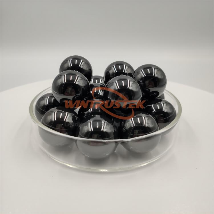
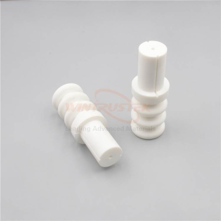
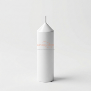
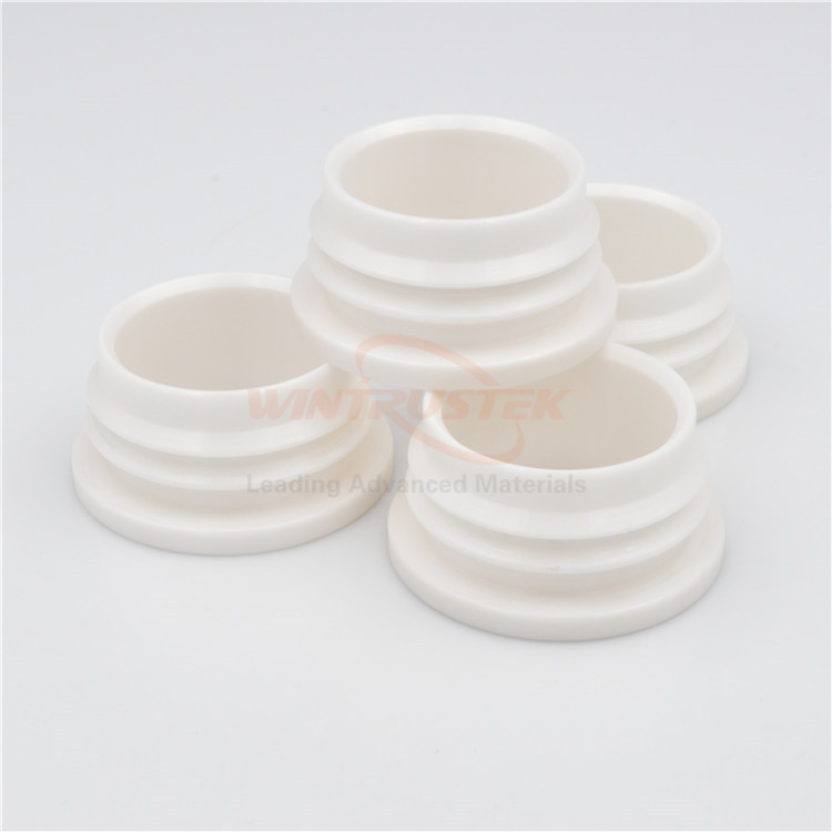
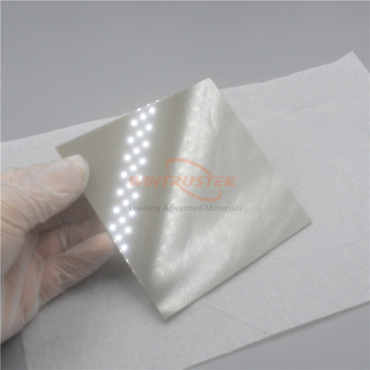
(AlN Substrate & BN Component Produced by Wintrustek)
In modern high-power electronics, semiconductor manufacturing and aerospace industries, power densities have surged. Today heat management has become the absolute determining factor for system stability, dependability and total lifespan.
Boron Nitride (BN) and Aluminum Nitride (AlN) are the two cornerstones of modern ceramics for demanding high-heat applications. Both combine strong heat conductivity with great electrical insulation in a unique way. However, their microstructures, mechanical properties and machining qualities are quite different.
To help you select the best material for your particular thermal difficulties, we will discuss four essential dimensions.
1. Thermal Conductivity: Heat Transfer in Isotropic and Anisotropic Systems
Both BN and AlN are excellent heat conductors. But they are very different in mechanisms and directions of heat conduction.
AlN has a hexagonal crystal structure of the wurtzite type and heat is transported uniformly by the lattice vibrations (phonons).
Commercially available high-density AlN ceramics have a stable thermal conductivity of 180 W/m·K to 200 W/m·K, which is about 5 to 7 times greater than that of conventional alumina (Al2O3) (theoretical limit 320 W/m·K).
Key benefit: AlN is fully isotropic, thus heat dissipates uniformly in all directions. This makes it the gold standard for planar heat sinks and substrates where homogeneous heat distribution is needed.
h-BN has a platy, layered structure akin to graphite and is often called “White Graphite.”Most of the industrial BN components are made by Hot-Pressing (HPBN). The compression of stacked platelets aligns them methodically leading to extremely anisotropic thermal conductivity.
The main advantage is that the heat conductivity in the direction of pressing is quite low (~30 W/m·K). But perpendicular to the pressing direction (along the crystal planes) it gets to 60-120+ W/m·K. (Note: The planar thermal conductivity of pyrolytic boron nitride (PBN) obtained by chemical vapor deposition (CVD) can be as high as 200–300 W/m·K.)
Selection Tip: If your application demands uniform, all-around heat distribution over a flat surface (e.g. LED or semiconductor substrates), AlN is your best choice. Alternatively, BN provides particular advantages if you have a very directional thermal route and your component demands complex mechanical geometries.
2. Electrical Insulation and Dielectric Properties
For power semiconductors and for Radio Frequency (RF) applications the material should be able to dissipate heat rapidly and endure high voltages without electrical breakdown.
AlN: extremely high breakdown voltage (usually >15–20 kV/mm), and extremely good in high-voltage high-current devices.
BN: Also has very good insulating properties (> 20-25 kV/mm). It is noted that BN still has a high electrical resistance even at the severe temperature of >1000°C and ultra-high vacuum.
BN Wins on RF: h-BN has a low dielectric constant (~4) and an ultra-low dielectric loss tangent (~10-4). Therefore, it is the material of choice for high frequency, microwave and RF window applications where reducing signal distortion and energy loss is crucial.
AlN: Higher dielectric constant (~8.5–9). It is not the best choice for high frequency RF windows but it works very well for regular semiconductor packaging.
3. Machinability: The Ultimate Cost and Lead Time Factor
This is the area where the two materials differ most significantly, having a substantial impact on your costs and delivery times for bespoke manufacturing.
The graphite-like layered structure of h-BN is inherently soft (Mohs hardness 2–3) and permits the crystal planes to split easily under cutting forces.
The Advantage: No diamond grinding needed. BN It can be easily machined, milled, drilled and tapped with standard high speed steel or carbide tools. This makes BN very cost effective for very complicated geometries, quick prototyping and for non-standard bespoke components.
AlN is a thick, covalently bonded compound with a high hardness (Mohs hardness 7-8).
The Downside: AlN components are very stiff after sintering. Tight tolerances or intricate geometries require lengthy diamond grinding, laser cutting or ultrasonic machining. This greatly increases production costs and lead times for complex, custom machined items Hotel.
Selection Tip: If your component design is complex or in the R&D/prototyping stage when you expect to make frequent revisions, BN will save you huge amounts of time and resources. If you design simple plates or blocks that can be mass manufactured by net-shape sintering, AlN is very cost effective.
4. CTE (Coefficient of Thermal Expansion) Matching
In high power packages, the ceramics must be securely interfaced to semiconductors (Si, SiC, GaAs) or metals (Copper, Aluminum) without failure during intense thermal cycling.
AlN’s Synergy in Semiconductors: AlN has a Coefficient of Thermal Expansion (CTE) of 4.5x10⁻⁶/K which is a great match to Silicon (Si) and Gallium Arsenide (GaAs). AlN expands and contracts at almost the same rate as the chip and so removes interfacial thermal stress which prevents delamination or die cracking.
Variable Expansion of BN: BN has distinct coefficients of thermal expansion in its various axes, making thermal matching with semiconductor dies more difficult to engineer.