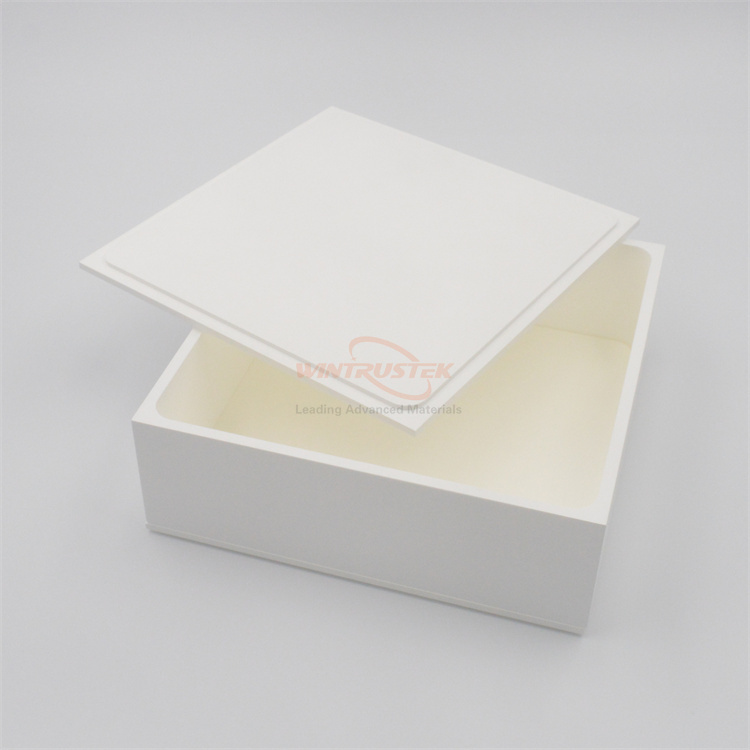
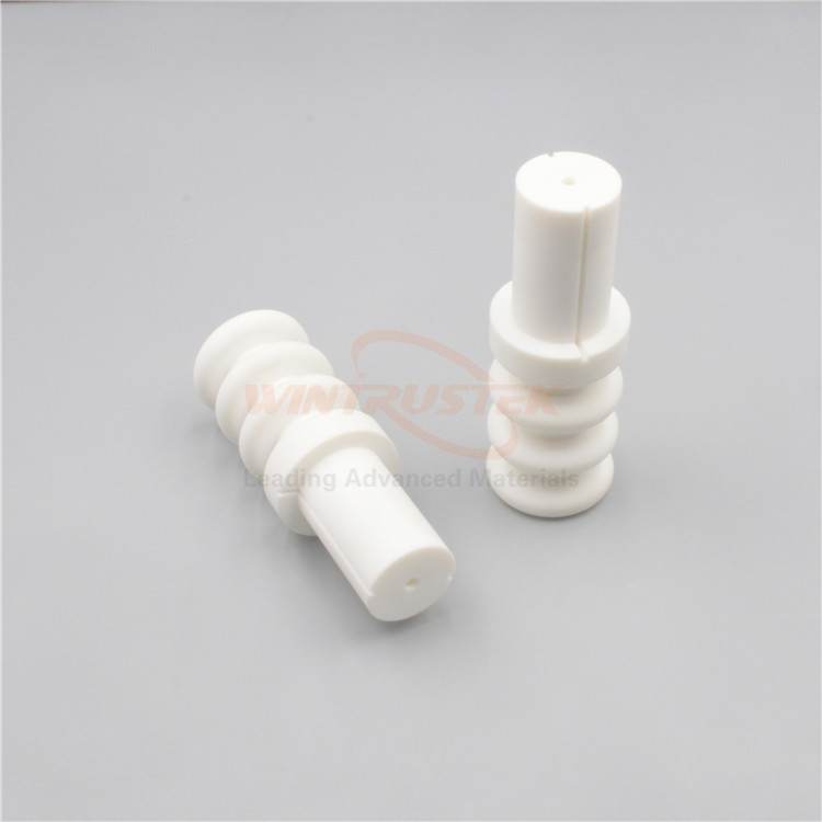
(PBN Crucibles Produced by Wintrustek)
In semiconductor crystal growth, molecular beam epitaxy, OLED evaporation, and high-purity material processing, a crucible is not just a container. It can directly influence material purity, thermal field stability, evaporation uniformity, crystal defect control, and long-term equipment reliability. That is why PBN crucibles have become an important class of advanced ceramic components in high-end manufacturing and research applications.
1. How Are PBN Crucibles Made?
Unlike conventional sintered ceramic crucibles, PBN crucibles are generally produced through a chemical vapor deposition process.
In simple terms, boron- and nitrogen-containing precursors react under controlled high-temperature conditions. The material is deposited layer by layer onto a mandrel or substrate until the required crucible shape is formed.
Compared with conventional sintered BN, PBN offers several advantages:
High purity for semiconductor and vacuum evaporation processes.
Dense structure to help reduce outgassing at elevated temperatures.
No sintering additives, which can reduce the risk of external contamination.
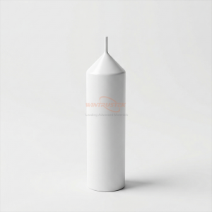
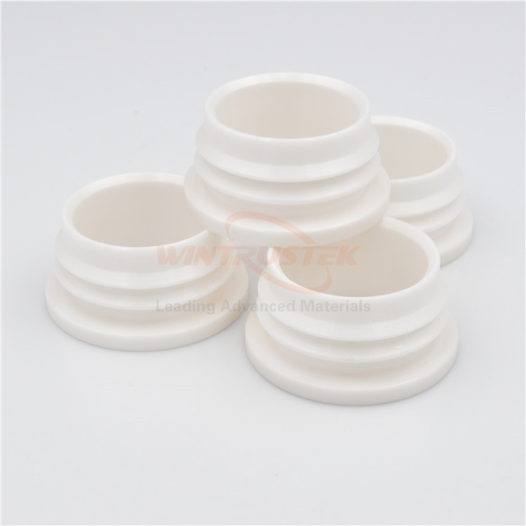
Customizable geometry for VGF, LEC, MBE, OLED, and other process designs.
2. Types of PBN Crucibles, Processes, and Applications
2.1 PBN VGF Crucibles
VGF stands for Vertical Gradient Freezing.
It is commonly used for the growth of compound semiconductor single crystals, especially materials such as GaAs and InP. In this process, raw materials are loaded into a crucible, melted under controlled conditions, and then gradually solidified along a vertical temperature gradient.
Because of this, the crucible material must offer high purity, stable thermal behavior, and reliable dimensional consistency.
Straight cylindrical crucibles for general material loading and crystal growth.
Conical-bottom crucibles to support seed crystal area design.
Seed-well crucibles to help control nucleation and growth direction.
Long-body crucibles for growing crystal ingots with specific length requirements.
High purity
Good thermal stability
Low outgassing
Customizable structure
GaAs single-crystal growth
InP single-crystal growth
Ge crystal growth
III-V compound semiconductor crystal growth
Crystal growth experiments requiring high purity and stable thermal fields
2.2 PBN LEC Crucibles
LEC stands for Liquid Encapsulated Czochralski.
This process is widely used for III-V compound semiconductor single-crystal growth, including GaAs and InP. Unlike conventional Czochralski growth, LEC uses a liquid encapsulant to cover the melt. The encapsulant helps suppress volatile component loss and maintain a stable growth environment.
In LEC growth, the crucible must withstand molten semiconductor materials, liquid encapsulants, long heating cycles, and demanding thermal field conditions.
PBN LEC crucibles are usually designed for larger melt volumes and stable crystal pulling conditions. Common design features include:
Large-volume structure for holding the melt and encapsulant.
Cylindrical or near-cylindrical shape to match crystal pulling systems.
High dimensional accuracy for stable thermal field control.
Thin-wall design with sufficient strength to balance thermal response and mechanical reliability.
Resistance to high-temperature melt environments
Reduced contamination risk
Suitability for larger crystal growth
Chemical stability
GaAs single-crystal growth
InP single-crystal growth
III-V compound semiconductor preparation
Semi-insulating crystal growth
High-purity metal or compound melting experiments
2.3 PBN MBE Crucibles
MBE stands for Molecular Beam Epitaxy.
It is a high-precision thin-film growth technology typically performed under ultra-high vacuum conditions. Source materials are placed in evaporation source crucibles and heated to generate molecular or atomic beams. These beams then deposit onto a substrate to form high-quality epitaxial layers.
In an MBE system, the crucible is small, but its requirements are extremely strict. It must tolerate high temperature, maintain cleanliness, and avoid contaminating the source material or vacuum chamber.
Small size and high precision to fit MBE source cells.
Conical or cylindrical inner cavity depending on source material behavior.
Thin-wall structure for faster thermal response.
High surface cleanliness to minimize source contamination.
Customizable diameter and depth to match source loading volume and evaporation rate requirements.
Low outgassing for ultra-high vacuum
High purity for source material protection
High-temperature stability
Chemical inertness
III-V semiconductor epitaxy
II-VI semiconductor epitaxy
Quantum wells, superlattices, and heterostructures
High-purity metal source evaporation
Research-grade thin-film deposition
Compound semiconductor device development
2.4 PBN OLED Crucibles
In OLED display manufacturing, many organic light-emitting materials, hole transport materials, electron transport materials, and metal electrode materials are deposited by vacuum evaporation.
In this process, the crucible acts as the evaporation source container. It must heat the material steadily under high vacuum while supporting stable evaporation rate, low contamination, and uniform thermal distribution.
PBN OLED crucibles are usually designed to match specific evaporation source structures. Common features include:
Small or medium-sized container structure for evaporation source assemblies.
Cylindrical, cup-shaped, or special-opening designs to support evaporation direction and material utilization.
High dimensional accuracy for good heater compatibility.
Clean surface condition to reduce contamination of organic materials.
Good thermal response for stable evaporation rate control.
Suitable for high-vacuum evaporation
Friendly to sensitive organic materials
Stable heating behavior
Compatibility with precision evaporation sources
OLED organic material evaporation
OLED metal electrode material evaporation
Display panel evaporation equipment
CIGS thin-film evaporation
High-purity functional thin-film deposition
Vacuum coating experiments
2.5 PBN Crucible Boats
PBN crucible boats are typically used not for large-volume melts, but for holding powders, granules, small pieces, metal sheets, semiconductor materials, or evaporation source materials.
They are common in laboratory research, high-purity material processing, vacuum evaporation, small-batch sintering, atmosphere furnace treatment, and semiconductor material preparation.
Shallow tray shapes for powders or particles.
Long boat shapes for tube furnaces or horizontal furnaces.
Flat-bottom designs for stable placement and uniform heating.
Customized length, width, and depth for different furnace chambers or sample sizes.
Thin-wall lightweight designs for fast thermal response.
High purity
High-temperature resistance
Low reactivity
Flexible for R&D and small-batch processing
Semiconductor material heat treatment
High-purity powder calcination or sintering experiments
Metal and compound material evaporation
Vacuum furnace, tube furnace, and atmosphere furnace experiments
Small-batch material synthesis
Auxiliary containers for crystal growth
High-purity sample holding
Overall, PBN crucibles play an important role in high-purity, high-temperature, and vacuum processes. From VGF and LEC crystal growth to MBE epitaxy, OLED evaporation, PBN crucibles support process stability and product quality through high purity, low outgassing, heat resistance, and chemical stability.
In practical selection, the key is not only choosing PBN as a material, but matching the right crucible type and design to the specific process, temperature, atmosphere, source material, and equipment structure.