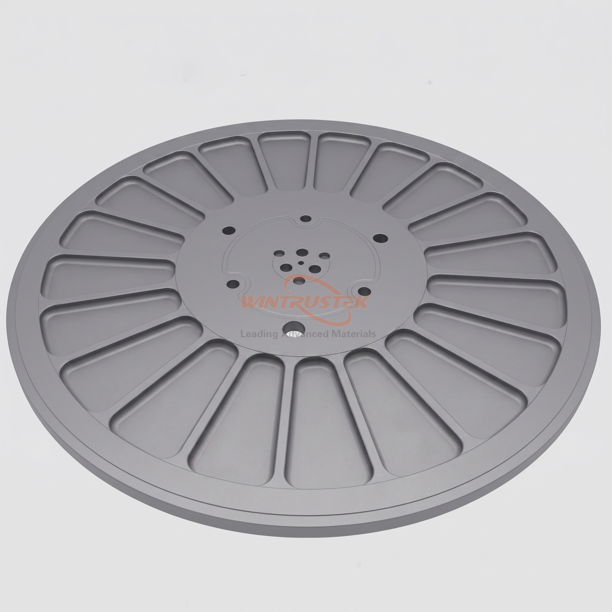
(SiC Wafer Susceptor)
In advanced semiconductor manufacturing, wafer processing stages such as Plasma-Enhanced Chemical Vapor Deposition (PECVD), Atomic Layer Deposition (ALD) and Reactive Ion Etching (RIE) are performed under severe circumstances. These high-vacuum reaction chambers are subjected to constant exposure to reactive plasma, corrosive fluorinated and chlorinated gases such as CF4, NF3, Cl2 and localized high temperatures > 500 °C.
In these hostile settings, standard metals such as stainless steel or anodized aluminum degrade rapidly leading to chamber corrosion, particle production, and catastrophic wafer yield loss.
Advanced technical ceramics provide the backbone for equipment engineers for continuous operation and sub-nanometer process reproducibility. High-Purity Alumina and Silicon Carbide (SiC) materials provide the ultimate in plasma erosion and chemical corrosion protection.
Wintrustek manufactures precision ceramic components that can survive the most severe Etch and CVD chamber conditions. Here’s a closer look at the role advanced ceramics play inside semiconductor equipment and the effect of material selection on tool life.
1. The Threat: Plasma Erosion and Chemical Corrosion in Chamber Tools
In conductor/dielectric etch and deposition cycles, chamber hardware is subjected to reactive plasma species in two damaging ways:
Physical Sputtering: Energetic ions (Argon, Fluorine or Chlorine ions) impact chamber surfaces pushing atoms off structural components.
Chemical Reaction: Reactive radicals form volatile metallic halides or non-volatile particle flakes on chamber metals that contaminate sensitive silicon wafers.
In sub-3nm node manufacturing, a small particle that falls onto a wafer can ruin numerous microchips. Therefore, chamber materials must have very low plasma erosion rates and zero particle production.
2. High-Performance Ceramic Solutions for Etch and CVD Tools
Different areas in the chamber require specific ceramic formulas to handle the varied thermal, electrical, and plasma stress profiles.
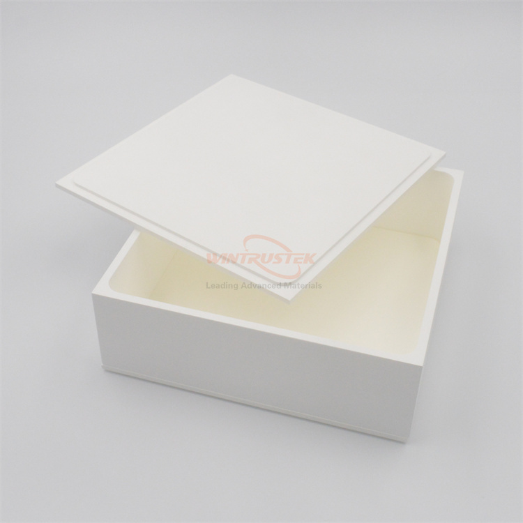
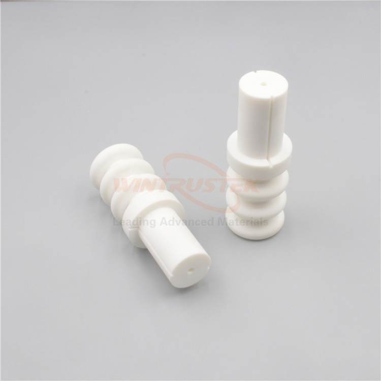
A. High-Purity Alumina (Al2O3): High-Voltage Isolation and Plasma Focus Rings
Properties: High dielectric strength, high mechanical rigidity, high fluorine plasma resistance.
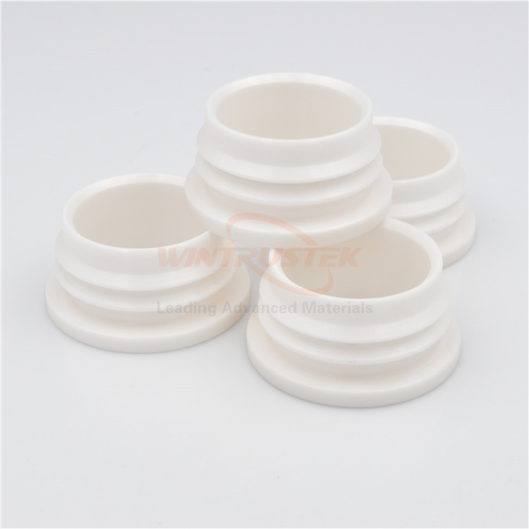
Applications: Electrostatic chuck (ESC) dielectrics, high voltage insulator rings, plasma focus rings, and RF feedthrough insulators.
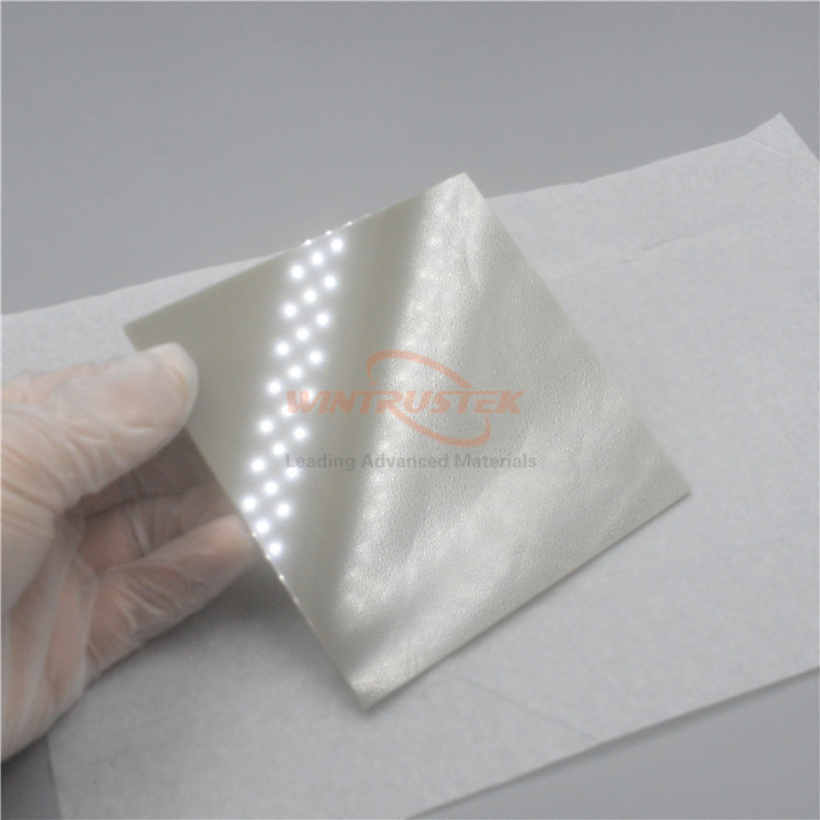
Wintrustek Capability: We provide high-purity Alumina components with 99.8% ground to submicron flatness to prevent electrical arc discharge in high power plasma chambers.
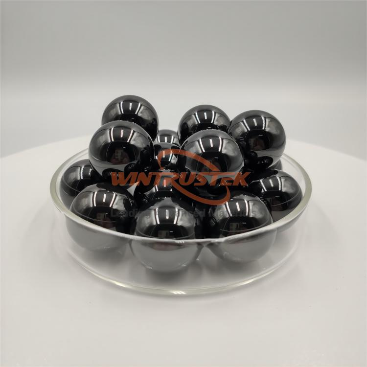
B. Silicon Carbide (SiC): High Thermal Conductivity and Plasma Resistance
Properties: Exceptional thermal conductivity, extreme hardness, low thermal expansion, and outstanding resistance to halogen-based plasma.
Applications: Susceptors, gas distribution showerheads, edge rings, and chamber liners.
Performance Gain: SiC components eliminate particle generation caused by thermal cycling mismatch, outperforming traditional quartz and anodized aluminum by orders of magnitude.
Upgrade Your Semiconductor Equipment Components with Wintrustek
As semiconductor manufacturing scales to sophisticated gate-all-around (GAA) architectures and 3D NAND stack counts go above 300 layers, chamber environments will become even more aggressive.
Wintrustek works with semiconductor equipment manufacturers (OEMs) and fab maintenance teams to provide precision-machined, high-purity ceramic components. Our products include custom ground SiC susceptors and Alumina ESC components with the goal of minimizing maintenance downtime and maximizing wafer yields.
Contact Wintrustek today at sales@wintrustek.com to speak with our ceramic engineers and request technical specifications for your semiconductor processing tools.