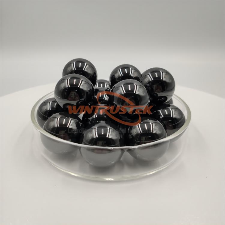
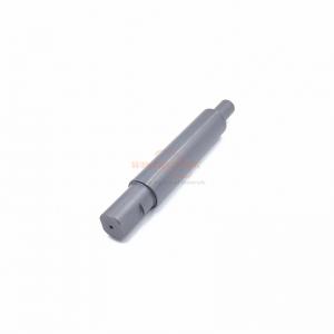
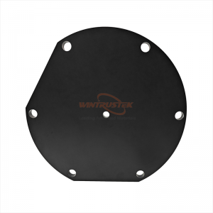
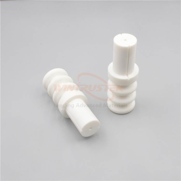
(PBN Products Produced by Wintrustek)
In the field of advanced ceramic materials, the fabrication route has a direct impact on material purity, density, microstructure, and final application performance. Chemical Vapor Deposition (CVD) is one of the key technologies for producing high-performance ceramics, valued for its high purity, strong process controllability, and excellent consistency in demanding industries such as semiconductors, vacuum coating, and crystal growth.
Pyrolytic Boron Nitride (PBN) is a representative product. With its high purity, high-temperature resistance, electrical insulation, low outgassing, and chemical stability, PBN is widely used in high-cleanliness, high-temperature, and high-vacuum environments.
1. Basic Principles of Chemical Vapor Deposition
CVD is a process in which gaseous precursors are introduced into a reaction chamber and, under elevated temperature or controlled reaction conditions, form a solid material on a substrate surface through chemical reaction or thermal decomposition. Unlike conventional powder-based ceramic processes, CVD enables layer-by-layer growth from the gas phase, offering clear advantages in purity, structural uniformity, and performance stability.
2. Key Characteristics and Advantages of CVD Technology
High Purity
Excellent Density and Uniformity
Strong Process Controllability
Suitability for Complex Shapes and High-Performance Components
Superior Material Performance
3. Application of CVD in PBN Preparation
PBN is a high-purity boron nitride material produced through CVD using boron- and nitrogen-containing precursors under high-temperature conditions. Compared with conventional hot-pressed boron nitride, PBN offers clear advantages in purity, density, and microstructural control, especially for critical components used in high-vacuum, high-cleanliness, and high-temperature environments.
Because PBN is typically produced without sintering additives, it is well suited for applications with extremely strict cleanliness requirements. Supported by CVD technology, PBN has become one of the most valuable and technically demanding products in the advanced ceramics sector.
4. Core Material Properties of PBN Products
One of the most notable advantages of PBN is its exceptionally high purity. Since it is produced through vapor deposition, metallic impurities and sintering residues are minimized, which is essential for semiconductor and vacuum applications.
PBN offers strong thermal stability and can operate for extended periods in high-temperature environments under vacuum or inert atmospheres. This makes it an ideal material for evaporation systems, crystal growth, and thermal field components.
PBN has high electrical resistivity and excellent insulating properties, making it suitable for electronic and semiconductor-related components that require both insulation and thermal stability.
PBN exhibits strong chemical stability against many corrosive environments and is less likely to react with process media, helping maintain system cleanliness and process consistency.
In vacuum systems, outgassing behavior directly affects process stability. Due to its high purity and dense structure, PBN generally exhibits low outgassing and excellent compatibility with high-vacuum environments.
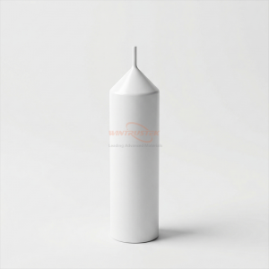
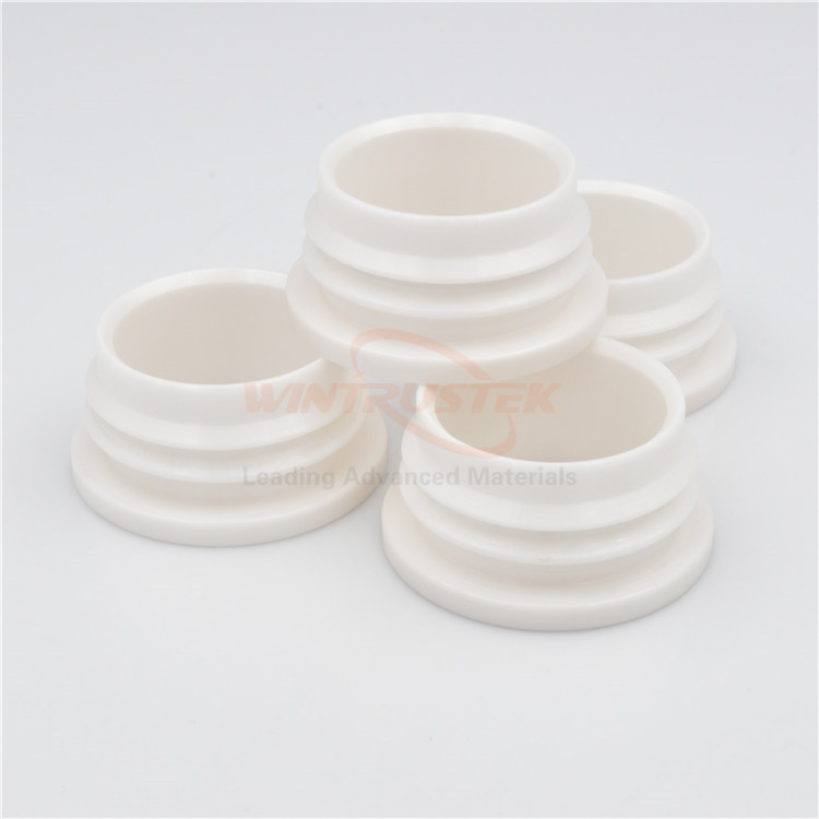
PBN can be manufactured into various forms, including crucibles, rings, plates, insulators, and evaporation components, to meet the dimensional and functional requirements of advanced equipment.
5. Typical Application Scenarios of PBN Products
In semiconductor processing, material purity and cleanliness are critical. PBN is commonly used in crucibles, insulators, and high-temperature components for equipment such as MBE, MOCVD, and vacuum evaporation systems, where contamination control and process stability are essential.
In OLED organic material deposition, source components must withstand high temperatures while maintaining ultra-low contamination levels. PBN is widely used in evaporation crucibles and related parts to support stable and consistent deposition performance.
In the growth of compound semiconductors, single crystals, and specialty crystals, PBN is often used in crucibles and thermal field-related parts, helping maintain chemical stability and material purity in high-temperature environments.
Because of its combination of thermal stability, low outgassing, and electrical insulation, PBN is suitable for key ceramic parts used in vacuum furnaces, electron beam systems, and other high-temperature vacuum equipment.
6. Conclusion
CVD technology provides a strong technical foundation for the development of advanced ceramic materials due to its high purity, strong controllability, and excellent structural characteristics. PBN products fabricated by CVD further transform these process advantages into material performance advantages, demonstrating significant value in high-temperature, high-vacuum, and high-cleanliness environments.